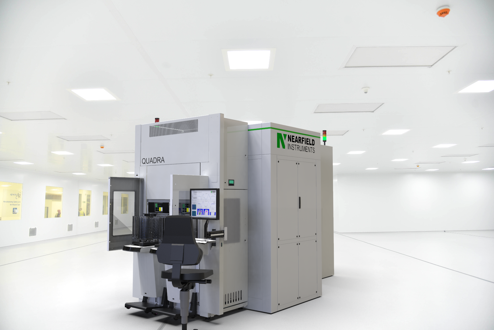
Nearfield Instruments High-speed data handling for metrology
Circuits on semiconductors are currently only a few nanometers high and wide. It is a huge challenge for producers to carry out quality measurements on this small scale. Nearfield Instruments has developed a revolutionary scanner that can do this. Technolution Advance contributed to the system integration and realized technology for high-speed acquisition and high-speed transport of data.
Scanning Probe Microscopy
Scanning Probe Microscopy (SPM) is a technology used to map surfaces at nano scale. SPM works with minuscule levers with a scanning probe that is only a few atoms large. This is used to scan the surface of the semiconductor wafer. The forces that occur between the probe and the wafer surface form the input for the measurement.
Disadvantages of SPM
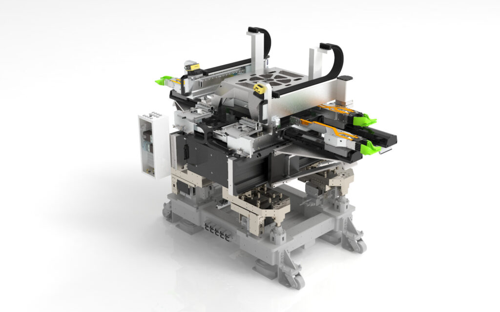
SPM has a number of disadvantages: the scanning speed is low and the point of the probe breaks easily. The greatest drawback is that the scanning probe damages the surface of the wafer. The solution developed by Nearfield Instruments (NFI) removes these difficulties: the technology is non-destructive, which means that the wafer is not degraded by the scan. Moreover, the scanner is much faster than the older solutions. NFI’s metrology system employs four scanning probes that scan the wafer surface concurrently, increasing the speed even further. Together with NFI, Technolution Advance is looking into further developments and improvements for future scanners.
High-speed data acquisition and high-speed data transport
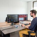
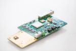
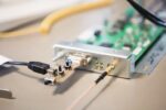
Technolution Advance was involved in setting up the architecture and in implementing, designing and integrating the many subsystems and operating elements for the high-speed data acquisition, the high-speed data transport and the operation of the scanning probes. We worked together very closely with NFI to solve the complex electromechanical puzzle of the scanning probes in the core of the machine. As space was strictly limited, we used very small prints and flex prints.